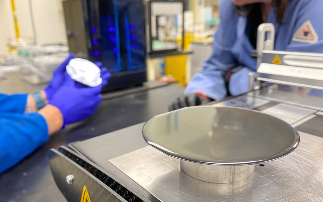
Current processes to make solar cells and power electronics have a manufacturing waste problem: up to 95% of the initial block of material, known as a wafer or substrate, is destroyed when wafers are extracted from the substrate then thinned out. These semiconductor manufacturing processes are called wire sawing and backgrinding.
Mariana Bertoni, a professor of electrical engineering in the Ira A. Fulton Schools of Engineering at Arizona State University, and her former doctoral student Pablo Guimerá Coll sought to reduce the waste from wafer manufacturing. They developed a precise method to apply a crack to the semiconductor substrate material with a small amount of force, then use sound waves to accurately guide the crack to cut off only the needed amount.
The resulting clean and accurate cuts allow the substrate material to be used multiple times and eliminate the need for backgrinding altogether, ultimately reducing waste in the manufacturing process.
“I’ve always been fascinated by the process of spalling, even in nature, and the role of vibrations in breaking things,” Bertoni says.
This fascination with vibrations and spalling, a process in which a piece of material is broken off from a larger chunk, resulted in Bertoni and Coll’s manufacturing method, which they dubbed “Sonic Lift-off.” After Sonic Lift-off showed promise, Bertoni and Coll founded Crystal Sonic in 2018 to further develop and commercialize their research.
Bertoni now serves as the company’s chief technology officer, while Coll has since graduated with his doctoral degree in materials science and engineering and is now Crystal Sonic’s research and development director.