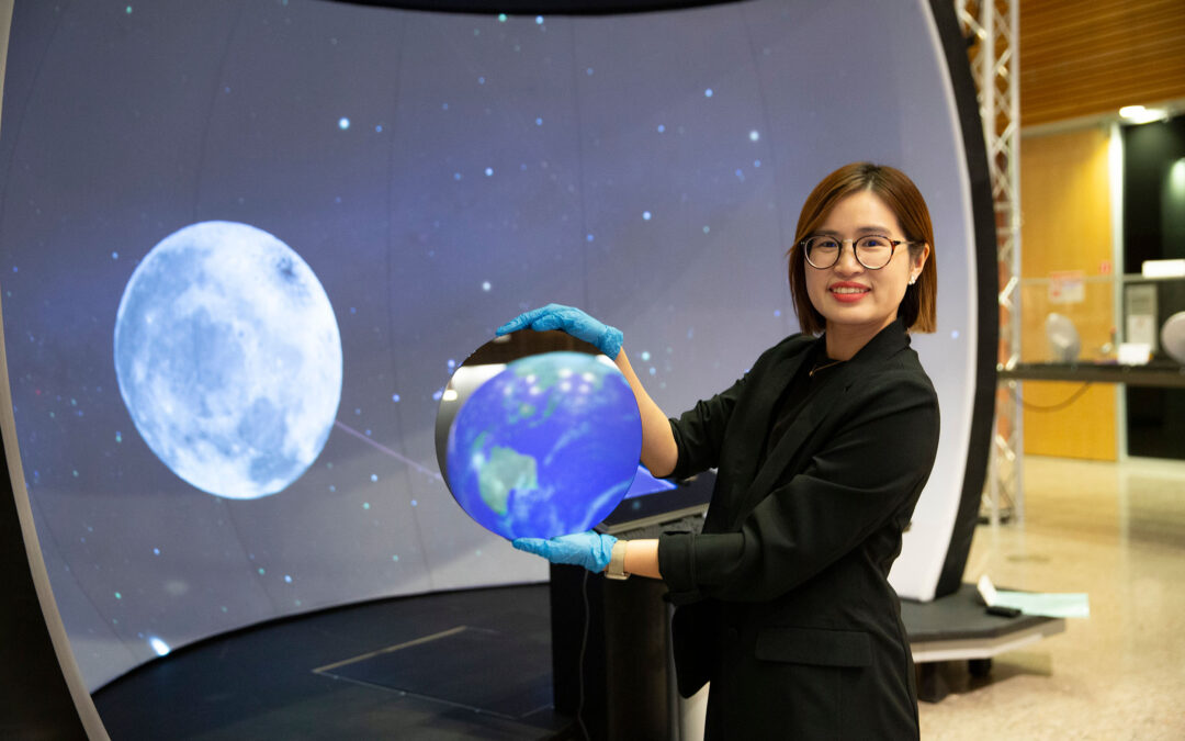
Factories floating in space sound like science fiction, but they may not be far off in the future. Ying-Chen “Daphne” Chen, an assistant professor of electrical engineering in the Ira A. Fulton Schools of Engineering at Arizona State University, is working as a co-primary investigator on NASA research with academic and industry collaborators to build a blueprint for building semiconductor devices in space.
Manufacturing microelectronics in space has the potential to eliminate key lengthy and costly steps in the semiconductor manufacturing process, specifically for 3D oxide-based resistive random-access memory, or RRAM, devices used on Earth. These 3D devices differ from traditional 2D RRAM devices by stacking layers of memory storage cells vertically instead of a traditional flat arrangement, allowing for a smaller footprint and more memory storage in a single device.
The team’s research is financed by funds from the CHIPS and Science Act and NASA’s In Space Production Applications program. Led by Principal Investigator Curtis Hill, a senior materials engineer at NASA, the project intends to harness the reduced pressure from microgravity in space to eliminate the need for etching, a step in which trenches are deepened in a chip’s surface to make sufficient room for its conductive metal contacts.
Etching is required in Earth-based semiconductor manufacturing processes due to the need for a thicker layer of semiconductor wafer thin film material to compensate for pressure from gravity. The researchers hypothesize a slimmer thin film layer can be used in space due to the lack of gravity, resulting in a trench already made deep enough during manufacturing to render etching unnecessary.
“To manufacture a chip, companies normally need many steps in a clean room on Earth,” says Chen, a faculty member in the School of Electrical, Computer and Energy Engineering, part of the Fulton Schools. “The goal for this project is to realize ‘all-in-one’ printing with a printer capable of manufacturing 3D stacking structures, active layers and metals.”
