After the coronavirus pandemic disrupted global supply chains in 2020, a shortage of semiconductor chips developed just as demand for consumer electronics increased from a population stuck at home. At the same time, international tensions increased between China and Taiwan, which produces the majority of the world’s chips.
Electronic chips are essential to international security as well for use in missile systems, fighter jets, tanks, radio communications equipment and more. To meet these needs and more, the U.S. government passed the CHIPS and Science Act, which provides $52.7 billion in funding for U.S.-based semiconductor research, development and manufacturing.
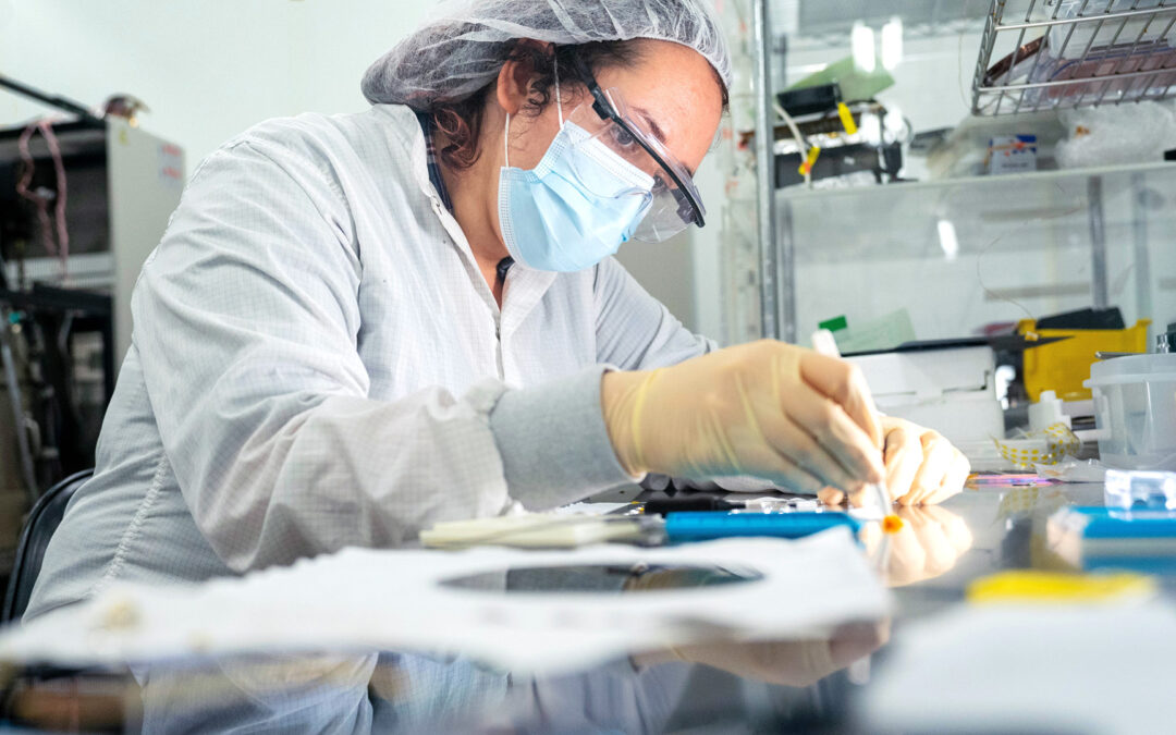
Provisions in the CHIPS and Science Act sponsored the creation of eight Microelectronics Commons Hubs around the country. The hubs aim to boost electronic innovations to advance experimental technology to production for the U.S. Department of Defense, ensuring powerful ideas make it beyond the research lab and into military equipment, while also growing a domestic semiconductor industry workforce.
One of these eight hubs is the Southwest Advanced Prototyping, or SWAP, Hub, an Arizona State University-led research and workforce development consortium of more than 130 partners from academia, government and industry. Hub partners include Sandia National Laboratories, Applied Materials, Northrop Grumman, Intel, NXP Semiconductors and the University of Colorado Boulder.
“The hub is supposed to create an ecosystem,” says Krishnendu Chakrabarty, Fulton Professor of Microelectronics in the Ira A. Fulton Schools of Engineering at ASU and the SWAP Hub’s chief technology officer. “It’s not just about ASU; it’s about the entire country.”